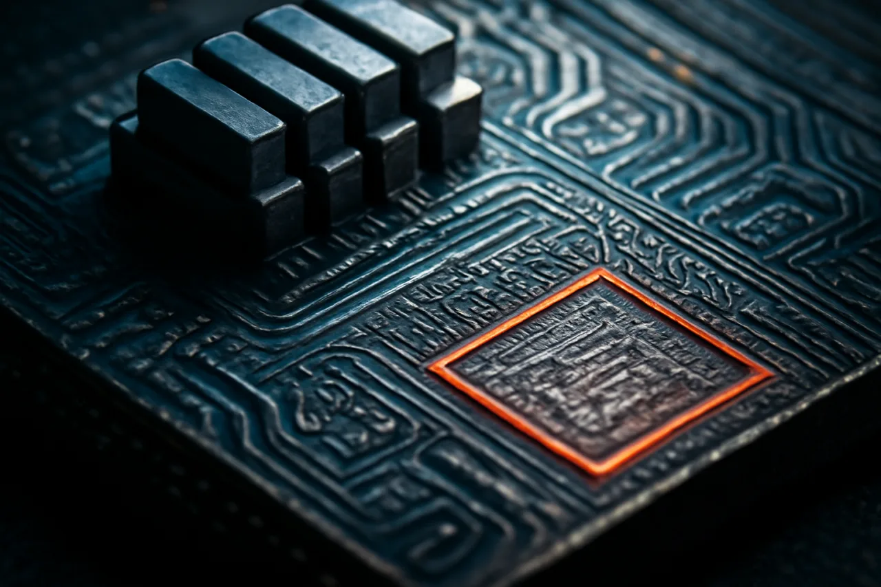
Samsung has succeeded in vertically stacking transistors with its 3D Stacked FET technology. This innovative architecture could provide radical gains in artificial intelligence and high-performance computing (HPC) chips. The three-dimensional arrangement of transistors not only increases area efficiency but also has the potential to reduce energy consumption, making it a critical element in the chip designs of the future.
What happened?
Samsung has taken a significant step in chip manufacturing by announcing its 3D Stacked FET technology. This technology promises to offer greater processing power and data processing capacity by allowing transistors to be stacked vertically. Instead of the traditional planar arrangement, this new architecture could enable more efficient use of space and reduced energy consumption.
Why is it important?
High-performance artificial intelligence applications and data centers are facing an increasing demand for processing power. Traditional chip architectures are struggling to meet these demands. 3D Stacked FET promises to fill this gap. In recent years, chip manufacturers have been turning to new architectures to provide greater area efficiency and power savings. For example, TSMC's FinFET technology offered the ability to house multiple processing units in the same area, but Samsung's 3D architecture could further intensify competition in this field.
Moreover, this new technology could pose a threat to rival companies. Major players like TSMC and Intel are trying to maintain their market shares with existing chip architectures, while Samsung's innovation may force them to reconsider their strategies. Competition in the chip market is now shaped not only by performance but also by energy efficiency. Samsung's 3D Stacked FET technology could provide an advantage in this regard.
What is changing?
The 3D Stacked FET technology could change a paradigm in chip design. Not only will chips be more powerful, but they will also operate using less energy, reducing costs for data centers and artificial intelligence applications. This situation creates a significant opportunity for companies looking to develop more sustainable technology. Thus, next-generation chips that align with environmental sustainability goals could emerge.
| Features | Traditional Architectures | 3D Stacked FET Technology |
|---|---|---|
| Area Efficiency | Low | High |
| Energy Consumption | High | Low |
| Performance | Medium | High |
What's next?
In the future, it will be interesting to observe how 3D Stacked FET technology develops and how it is adopted by other major chip manufacturers. If Samsung can quickly integrate this technology into commercial products, it will increase its chances of becoming a significant player in the market. Other companies are also expected to develop innovations similar to this architecture. Additionally, it will be intriguing to see how such initiatives will accelerate developments in artificial intelligence and HPC.
In conclusion, Samsung's 3D Stacked FET technology has the potential not only to increase its own market share but also to create a transformation across the industry. This innovation could guide the future of chip designs and reshape competition.
Yorumlar (0)
Henüz yorum yok. İlk yorumu sen yaz.
Yorum yapmak için Sinyal'i indir
Yorumlar Sinyal hesabıyla yapılır. Mobil uygulamada giriş yap, yorum bırak.